Update: this project is evolving. See this page for the latest version. Kits are available in the shop area.
The announcement of the MRF300 and MRF101 transistors by NXP in 2018 has generated quite a spark of interest in the amateur radio community and as soon as I learned about them I wanted to get some on my workbench.
And of course they’re interesting: you get the latest LDMOS technology, they’re designed for medium-high power levels (where the offer is not as rich) and are being offered in affordable plastic packages. It almost hits the impossible “quick, easy and cheap” trifecta … if only there would be a design out there that amateur radio enthusiasts could use as a starting point for their projects. Well, with the article below we’re hopefully a step closer to that point.
This project is meant to demonstrate the capabilities of the MRF300 transistors as linear broadband devices in the 2-50MHz range and to be used by radio amateurs as a starting point for a medium-high power amplifier. This is also my entry to the NXP Homebrew RF Design Challenge 2019.
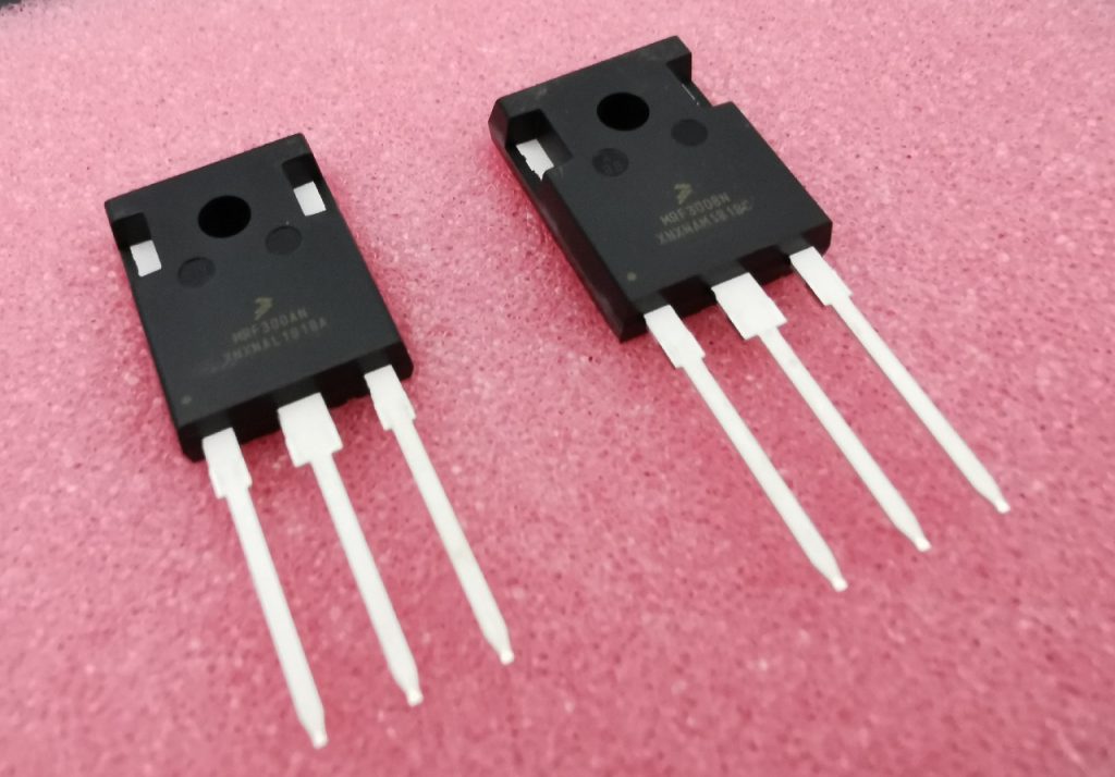
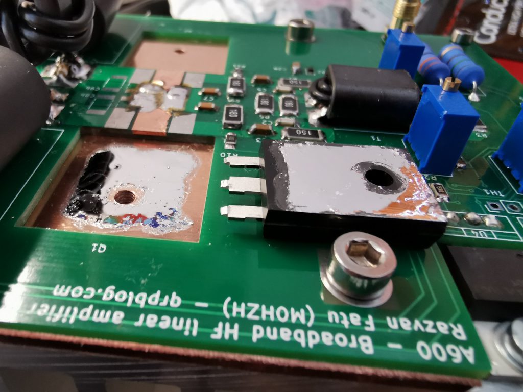
To achieve the target of 600W output while also minimizing the level of even-number harmonics, a “push-pull” configuration of two transistors is used. Luckily, the manufacturer made it easy to design the PCB layout for such a thing by offering two versions (the MRF300AN & MRF300BN) that have mirrored pinout. The common TO-247 package is used, with the source connected to the tab.
Each individual MRF300 LDMOS transistor is specified at 330W output over a 1.8-250MHz working frequency range, a maximum 28dB of gain and over 70% efficiency. The recommended supply range is 30-50Vdc. By studying the specifications, it looks like with correct broadband matching and some operational safety margin we can get close to 600W output at a voltage of around 45V across a resonably large bandwidth; the aim is to cover 1.8 to 54MHz.
Main challenges when designing this amplifier are related to achieving good input and output matching over the entire frequency range as well as maintaining high and flat gain. Good linearity and a low level of harmonic products are mandatory. As the TO-247 is not a package specifically designed for high-power RF, there are some challenges with thermal design and PCB layout as well.
Circuit Description
The circuit schematic can be seen below. For input a 4:1 transformer is used, along with a 33ohm resistor (R1) that partially dampens the reactive response and improves input matching.
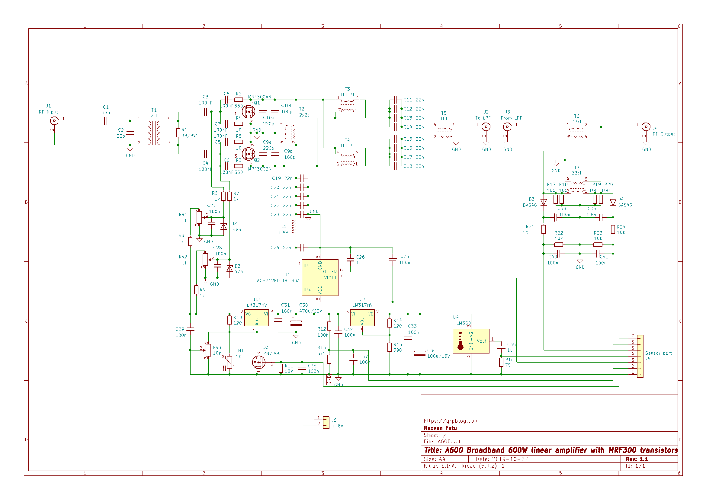
The idle current for the MRF300 LDMOS transistors is set at 300mA each, with a bias gate voltage of around 2.7V. To achieve this value, a LM317HV high voltage linear regulator takes the supply voltage and adjusts it down to a value around 8-10V, which is further divided down to the exact value via individual adjustable multi-turn potentiometers. A negative-coefficient thermistor is present in the regulator’s feedback loop so when the heatsink temperature increases the MRF300 gate bias voltage decreases slightly in order to maintain the same idle current. An external signal can cut off this voltage in order to reduce power consumption when the amplifier is not used.
The 560 ohm resistors (R2 and R3) provide negative feedback, making the amplifier more predictible in response and improving IMD performance. For a small increase in overall gain, it is worth investigating increasing their value.
Matching the output to 50ohm is where the real challenge is. For maximum efficiency across a large bandwidth, transmission line transformers (TLT) are the best option and the closest transformation ratios possible are 1:4 or 1:9. With 50V supply and a 1:4 transformer, the maximum output power that can be obtained is around 400W as the theoretical load impedance for each transistor is too high. With a 1:9 transformer higher power can be achieved but the matching becomes more critical; the supply voltage can be reduced below 50V in order to improve efficiency, but current needs to be actively monitored and kept in the safe area (below 20A in total).
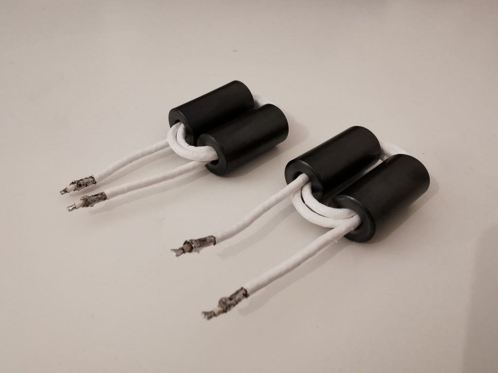
For minimal losses, the coaxial cable used in the TLT has to have a characteristic impedance that is the geometric mean of the input and output impedances. As this is a 1:9 transformer and the output has to be 50ohm, the input impendance works out as 50/9 = 5.56ohm and the coax characteristic impedance is sqrt(50*5.56) = 16.67ohm. I chose TC-18 coaxial cable specifically designed for this purpose, that has 17ohm impedance and uses high quality materials so it can handle high power and temperature. 3 lengths of RG-316 in paralel can be used as well in order to achieve the 17ohm impedance, but RG-316 is harder to work with and it might be a challenge to fit it 9 times within usual ferrite cores.
The length of coaxial is best kept short in order to maintain efficiency at high frequencies, ideally below 1/10 of a wavelength at the maximum frequency. 30cm is enough for 3 turns through the popular 26xx540002 bead ferrite cores from Fair-Rite and taking the ~0.7 velocity factor into account, it stays below that.
Choosing the ferrite core for the output transformer is key to achieve the best performance. The first prototype used Fair-Rite 2667540002 ferrite beads (material 67) in an attempt to achieve the widest working range possible with best efficiency; this sacrifices performance in the lower amateur radio bands, as below 10MHz there is a significant drop in efficiency. Laird 28B1020-100 cores have been tested as well, with relatively similar performance to the material 67 Fair-Rite cores.
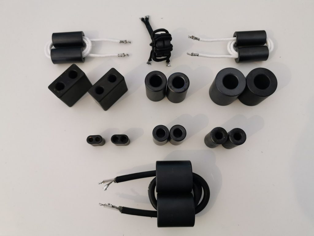
In the second design 2661540002 cores are used. Material 61 has higher permeability than 67 (125 vs 40), providing suffcient choking inductance at 1.8MHz even if it could become slightly lossy at higher frequencies. Material 43 (850ui) is a good candidate as well and should also be investigated.
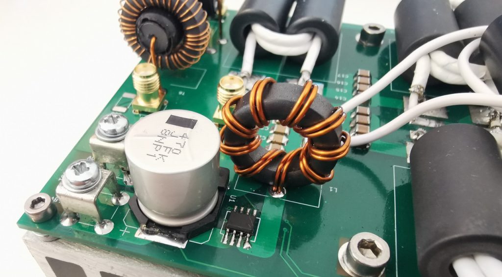
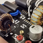
A 2×2 turn transformer built on a separate 2643540002 (material 43) core is used to supply DC voltage to the LDMOS’ drains. This proved a key component as well, as performance below 10MHz is affected by its configuration. The 1:9 output transformer is followed by a 1:1 choke BalUn that makes sure the output is rid of any common mode current.
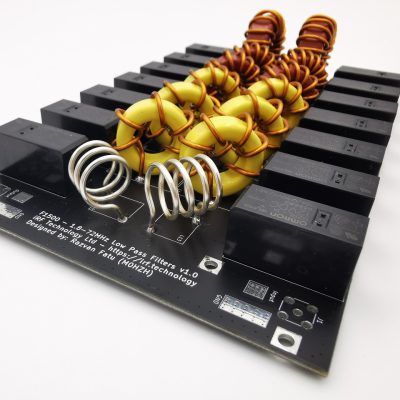
The board is fitted with two SMA connectors where a bank of low-pass filters can be inserted, in order to further diminish the harmonic contents at the output; as this is is not the purpose of this article, a straight jumper cable is installed instead.
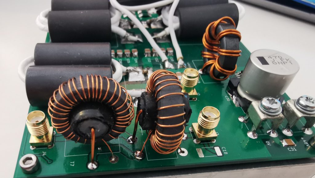
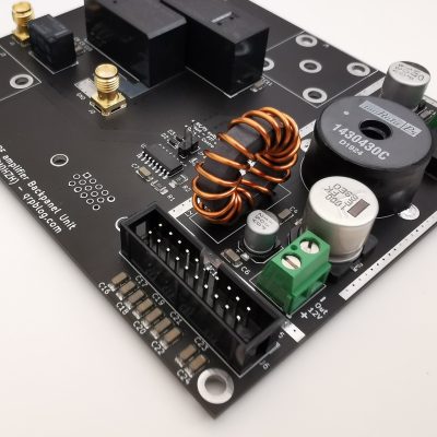
The output of the amplifier board includes a tandem coupler designed to measure the output and reflected power. The signals are provided via a 7 pin header connector, that also outputs a fraction of the main supply voltage, a current measurement (achieved with an ACS713 Hall sensor) and a temperature measurement (from a LM35D precision temperature sensor).
These signals can be used to measure the performance of the amplifier and can also be used to implement fast-acting protection logic for overvoltage, overcurrent, overheating, output mismatch etc with the help of additional circuitry.
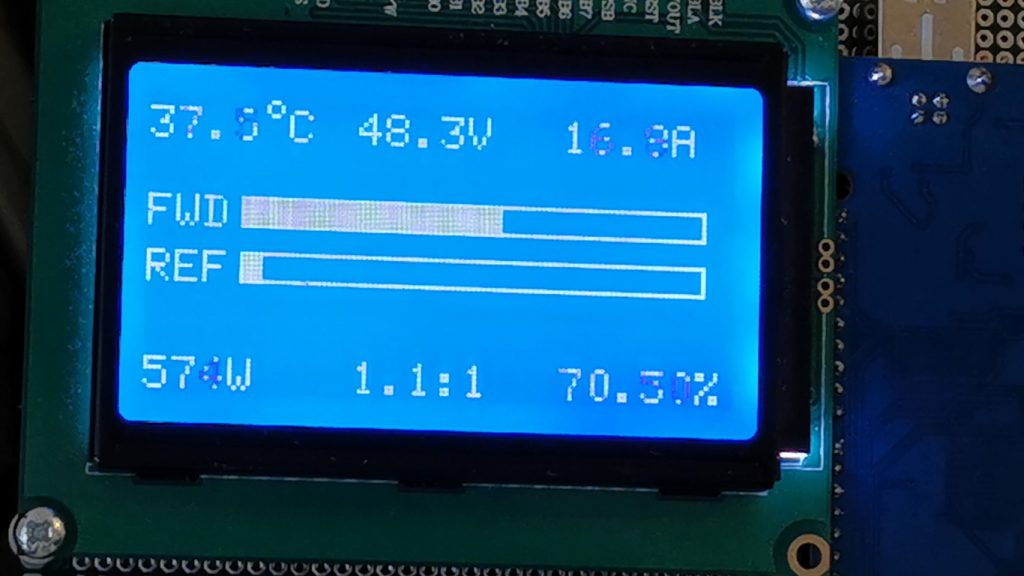
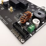
Above you can see the Arduino based monitoring tool that offers accurate measurement and has been used during the development of this circuit. Its precision has been verified against multiple industrial equipments and calibrated where necessary.
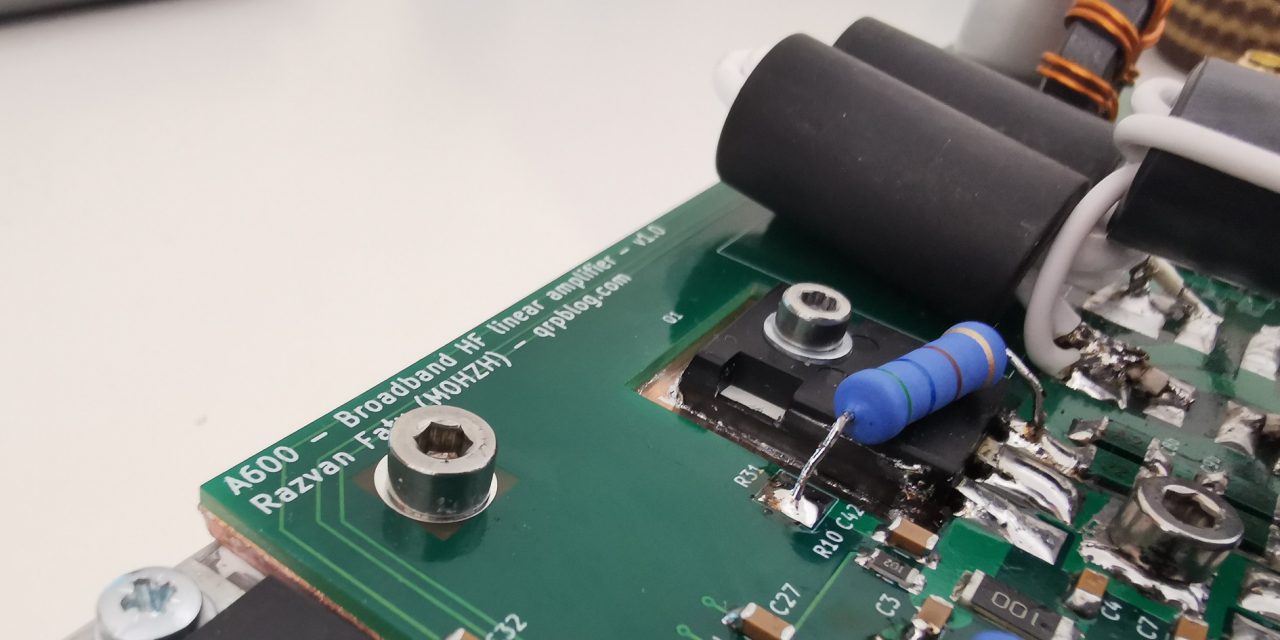
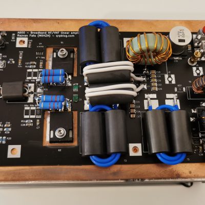
The Printed Circuit Board
With high-power RF devices, it is always important to have a very good, solid and continuous ground plane. Because the MRF300’s Source is connected to the tab, the heatsink will be used as a ground plane and the PCB is designed with that in mind; the bottom PCB layer is also used as a ground plane, as it comes in contact with the heatsink over a large area.
SMD parts are used where possible, in order to minimise stray inductance. The power traces are thick in order to support the high current and the RF traces have been sized for the right trace impedance where possible.
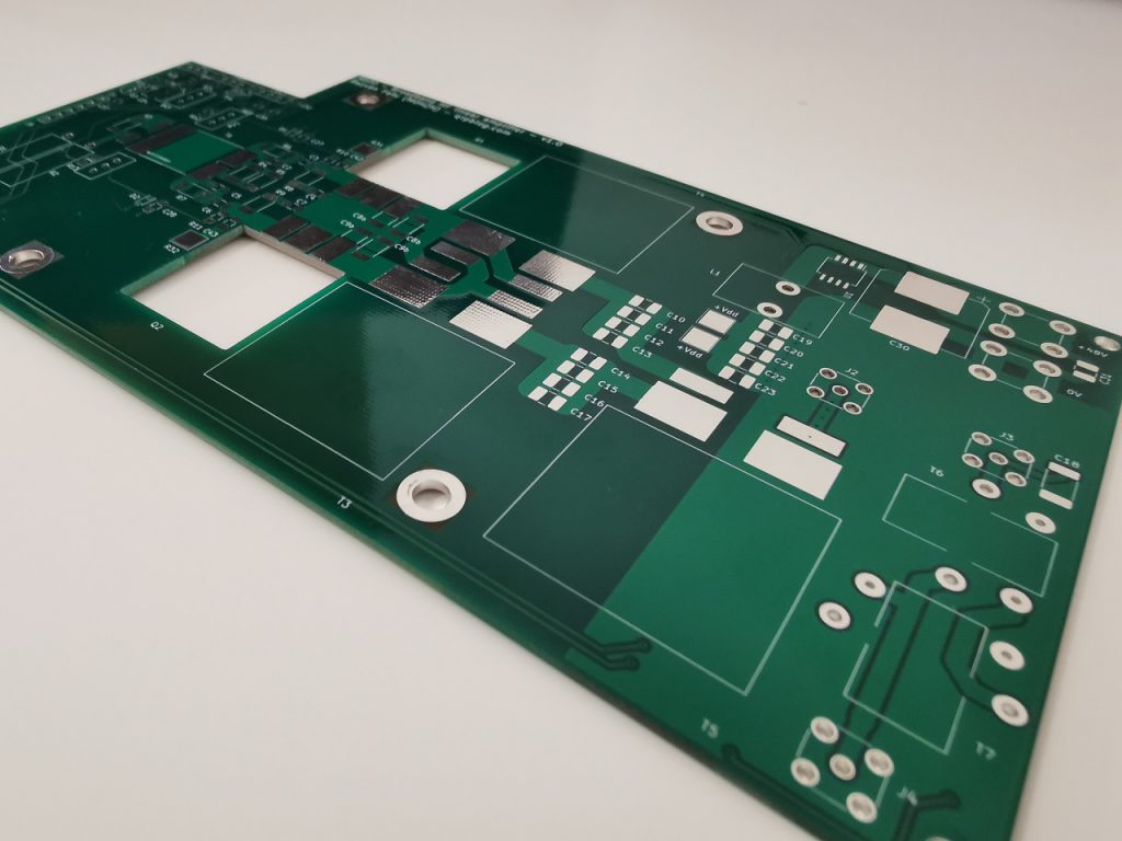
For the schematic and PCB design I’ve been using KiCAD, which is is good as it gets for free software; the files generated by KiCAD can then be sent to a PCB manufacturer. I have used PCBway for this, the process is as simple as creating an account and uploading your files (they have a quick guide on how to do this if you haven’t done it before). They check your files and send them to production and if you choose DHL delivery you could get the finished product in just a few days. Tip: if you manage to keep your PCB under 100x100mm, they only charge US$5 for 10 pieces (!). This is insanely cheap for hobbyists.
Thermal design
One of the critical points with high power transistor amplifiers is keeping them cool. The datasheet Mean Time To Failure (MTTF) for the MRF300 is about 70,000 hours for a current of 8.7A and a junction temperature of 175C, so the cooling system needs to keep the transistors below that temperature at all times. As the junction-to-case thermal resistance is 0.55C/W and we expect a maximum thermal dissipation of about 200W per device, this means the case temperature can’t go over 65C.
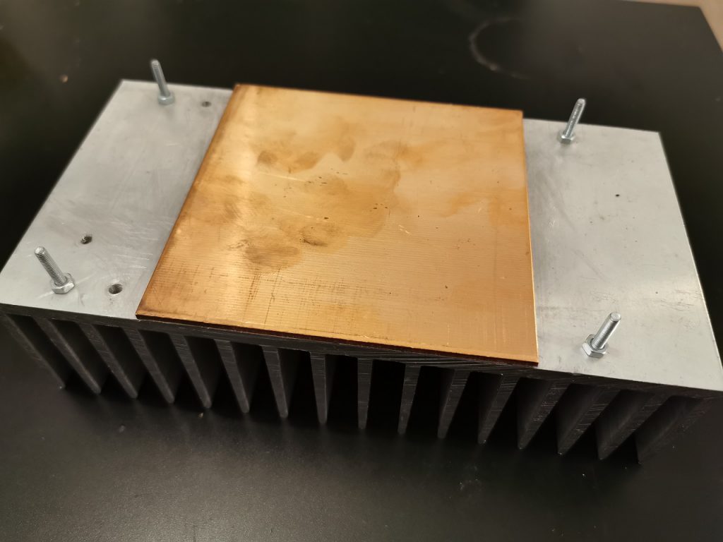
An intermediary 3mm thick copper plate is installed between the transistors and the aluminium heatsink, as copper has better thermal transfer properties and offers a path of lower resistance for the thermal energy from the two tiny (1.7 square centimeters) power transistors to the entire heatsink base.
To make sure we have minimal resistance transferring heat from the transistors to the copper plate, the surfaces have to be perfectly even & clean, enough pressure is applied and a Thermal Interface Material (TIM) is used. Usually the TIM is a silicone-based grease that requires high pressure to be applied and is often electrically insulating; as we are using the heatsink as a ground plane as well, we want the electrical contact to be as good as possible. Alternatively, some transistors can be soldered directly to the copper plate, but this is a rather permanent process, requires a special oven for the best results and doesn’t really work with the MRF300’s TO-247 packaging.
My choice was to use the best of both worlds: metal, but liquid. More precisely, an eutectic alloy of soft metals (tin, gallium and indium) called Galinstan. Depending of the mix ratios, this alloy is liquid at room temperature, naturally adheres to other metals, offers exceptional thermal and electrical conductivity and doesn’t require much pressure to achieve best performance. The disadvantage is it is expensive, corrodes aluminium agressively and it’s a bit difficult to contain. Luckily, you can find it in a few commercial flavours as a computer cooling TIM that includes the kit necessary to apply it correctly. I chose Thermal Grizzly Conductonaut but I understand Coollaboratory Liquid Metal Pro is just as good. A totally unecessary better option would be pure Indium pads (like the Indium Heat-Spring), but these are much too expensive for this purpose and also quite difficult to source.
Assuming a conservative 0.1C/W thermal resistance from transistor case to the aluminium heatsink and an environmental temperature of 30C, the thermal resistance of the heatsink to air adds up to 0.0775 C/W (for both transistors, 400W dissipation in total). Heatsink manufacturers will provide this figure sometimes as a chart, depending on airflow. With the help of a microcontroller we can design a fan controller that will regulate the fan speed so it follows this chart and only reach 100% when temperature gets close to the limit (calculated here at 61C for the aluminium base). The heatsink’s thermal inertia can help keep sudden fan speed variations in check, so a larger copper base might be useful.
Machining the heatsink (and especially the copper plate) is challenging, as copper is soft and will load the drill bit until it gets stuck and breaks. The tricks are to use a cutting fluid and a slow speed; lard seems to be very good for lubrication and it really makes drilling much much easier, the brand I’ve used is Monument White Tallow Medium. Tapping the screw holes afterwards was easy, all it needs is patience. I had to be careful not to get TIM close to the bolts that hold the transistors down, as those reach the aluminium heatsink base and it would corrode it.
Test Setup
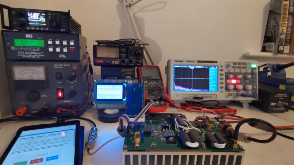
This is a homebrew project, so the test setup is pretty typical of a hobbyist’s test bench. Most of the equipment is not of lab-grade precision, but still accurate enough for amateur radio.
- Power supply: HP ESP120 3kW telecommunications PSU
- PSU for accessories: Daiwa PS-304
- Dummy load: MFJ-264 1.5kW 50ohm with -40dB output port
- Signal source: Xiegu G90 and Xiegu X5105
- Input power & SWR meter: MFJ-929
- Output power & SWR meter: Avair AV-600 (for measurements under 400W)
- Oscilloscope & FFT analyser: Hantek DSO5102P
- Multimeters: Uni-T UT61E, Uni-T UT31C, Amprobe 5XP-A
- VNA: nanoVNA (for testing input & output transformers and matching)
Measurements
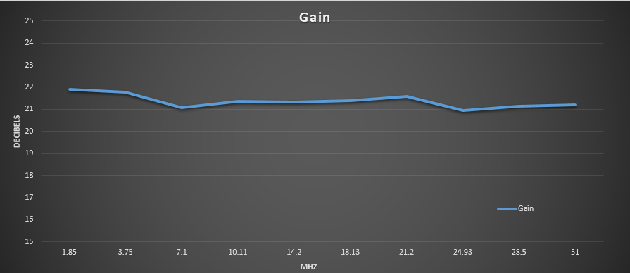
The results have been compiled into these charts:
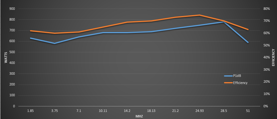
The amplifier is slightly under 600W (about 580W) at 3.7MHz (the 80m band) and works most efficiently in the higher bands. The highest output power I’ve measured was 840W (!) in the 10m band, but the wave was distorted and the harmonic levels were high. Around 750-780W the output is still clean enough, but it’s debatable if that’s a safe operating area.
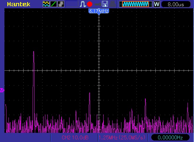
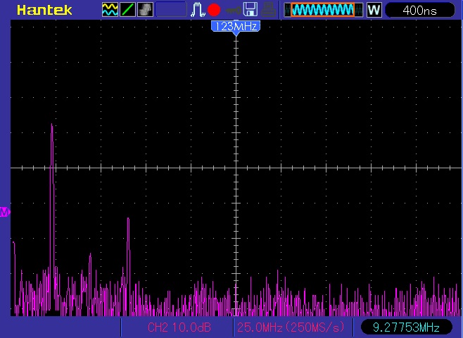
Without pushing it over the limit, the harmonic levels are quite low and close to what the signal source measures. Here are two examples below; keep in mind the measurement is in voltage, so for RF power the vertical scale is double (20dB/div instead of 10dB/div).
As a conclusion, I think these new devices are excellent. Leaving the performance aside, during the development of this amplifier I’ve abused this pair of transistors in many ways, including driving them into short and open loads, using them with sub-par cooling and massively exceeding the drain current. They’re still alive and well.
Want to make sure you don’t miss important updates on this project ? Sign up here:
Shop for kits:

Why not use the RD100HHF1 – about the same price, and commonly available. It can supposedly handle (by spec sheet) a 20:1 SWR at full load without damage. Yaesu has used them in a number of recent xcvrs, like the FT-950 and -2000.
RD100HHF1 are 12.5V 100W devices; MRF300 are 50V 300W devices. Very different animals.
Maybe I missed it… Are the circuit boards available (github or elsewhere?)
I am considering making this available as a kit. Stay tuned ;).
wait fot kit friend
At least a circuit board and bill of materials. This looks like a winner!
I’d be interested in a kit!
Nice work, thanks
I would be interested in a kit
Excellent write-up with valuable explanations! In so many amplifier builds the authors assume the readers know why they have chosen certain matching methods etc.
Interesting article and a nice write up, would certainly be interested in a full kit or just a board (supply own components) and look forward to future updates
Would love to see the 2 tone test results
Same here, 2-tone test results for linearity please!
Let us know when your list are to buy
Excellent production quality presentation.
Thanks for sharing.
73 de Claude – VE2YI
Razvan – put me on your mailing list !
73,
Jim WQ2H / WK2XAH
where’s Zenki’s comments?
Put me on your email list. Scott Cook KJ4NDQ
I would love to see this as a kit.
Interesting work. I noticed you mention 4:1 input but schematic says 2:1. A kit of parts / go fund me may be the way to go. I especially would be interested in bandpass design, to accommodate the required -45db supression required by US FCC standards. Finally Sensor port J5 not documented as to use and intent.
The schematic refers to the turns ratio, 2:1 turns equals 4:1 impedance transformation. A bank of low-pass filters is indeed necessary and might be the subject of another article.
The connector is indeed not documented, I will add a section about it soon. It’s mostly 0-5V analog signals with one 5V TTL input that kills the bias, it can interface directly with an Arduino.
Foarte interesant, si….INTERESAT.
Razvan, excellent engineering and write up. I am keen to construct similar. If you are thinking of sharing the gerber files I would be very interested.
73
Peter
What’s your sense about useful power out that could be got at 70 MHz, maybe drop 1.8 MHz, and use Fairite 43?
Haven’t tested 70MHz yet. The P1dB, efficiency and gain all drop a bit at 50Mhz so probably it will be even worse at 70MHz (450-500W out max ?); some adjustments will have to be made at the input and output circuitry to improve performance.
Well max in UK is 160 W so that would be fine so long as efficiency isn’t too bad
Good Initiative Razvan, and appreciate for a Very neat layout – just gone through the video. BTW. if you can provide the transformer details like the core part# you might receive valuable comments from the viewers as the Transformer further modification can bring up the efficiency.
keep me posted for the kits availability. If its just the PCB and PCB with parts will increase the # of users BECAUSE lots of people want to buy just the PCB in stage 1 and then the components because of various constraint. ALL THE BEST
Hi there , very interesting build and a quality pcb . Put me down for a kit when available . William GW4LWD
Interesting project. I did some experiments in the past with cheap mosfets from switching power supplies (IRF and IRFP types). In test setup with dummy load there was a lot of power but when the amp was connected to an antenna the amp was very unstable. I would like to see how this amp with MRF300’s behaves when delivering its power to an antenna. So keep on mind, a working prototype on your test bench is not the same as using it on air. Your antenna will have a bad reflection loss compared to the dummy load. Your antenna could also have an inductive or capacitive impedance and the amp will not like this. Anyway thanks for sharing this and good luck with your projects.
Thank you Mark. The MRF300 are not cheap switching PSU transistors, they are proper RF LDMOS transistors (lower rated, but similar to MRFX1K80, BLF188 etc) in more affordable packages.
This is quite an excellent design! It’s certainly the best and most well thought-out I’ve seen for this contest so far. Good luck! Perhaps consider open-sourcing the hardware design, it would be a great contribution.
I am working on some IRF510-based amplifiers, you can see them at http://github.com/profdc9/QRPAmplifier . It is also open-sourced under CC-BY-SA 4.0.
Thank you !
About the IRF510 amplifiers, I’ve had good results with a 15ohm /5W resistor in paralel with the input transformer’s secondary. This sacrifices overall gain but makes for very good input matching and flat response up to 30MHz.
Hi razvan. Nice write up. Interesting to try this one. How do i get the board? I would love to build of those.
Exceedingly nice work! I would love to build one of these when you have it ready. Please let me know when you have kits available, or put me on your email distribution list.
Kind regards and 73,
Glenn
Salut Razvan (cred ca ai deschis cutia Pandorei ) sunt interesat de acest montaj când ai un chit cit de cit complet da un semn de viață. Andrei
Hello!
Excellent job! But i’m looking for more mobile amplifier with 12 or 24 VDC supply. (like an Ameritron ALS-500). Is there a room for modification with your design ?
Thank you ! Unfortunately this a 45-50V design, you would need a high power DC-DC converter which would probably make it too complicated for what it wants to be.
Awesome design!
Confused by differences in schematic part labeling vs PCB; eg, R3 vs R31.
Thanks. The PCB was designed for an older version of the schematic (v1.0) an after a lot of testing I ended up with an improved v1.1, which is the schematic attached (that has different part references). In the mean time, further developments have produced v1.2, which goes back to the same references as v1.0 and you can find that here: https://qrpblog.com/a600-hf-6m-600w-ldmos-amplifier/
Thank you for this fine presentation. I will look forward to getting a board and/or kit. May I ask why you chose an SMA connector for J4? I would be worried about power handling with an SMA. Of course, it would be simple to change to any connector I might choose, such as an SO-239 or NF.
SMA is used for minimal insertion loss, minimal PCB footprint and wide compatibility. SMA connectors are rated for 600W continuous @ 1GHz, at HF they are limited by the insulation breakdown limit, which is typically around 300-350Vrms depending on who makes the connector. 600W is about 173Vrms, even with high SWR it’s hard to reach 300V and the SWR protection will shut down the amplifier well before that happens.
Would REALLY love to see this available in kit form! Along with detailed instructions. Great work, Razvan!
I read that the original TIM was corrosive to Aluminum. Is your substitute Aluminum-friendly, or still corrosive, but not to the copper spreader. NICE design!
It’s the Gallium in the liquid metal TIM that corrodes Aluminum, that’s one of the reasons I’ve used a Copper heat spreader in between.
Please put me on your mailing list also if you don’t kit could you let me know what core is T5 and about how much TC18 coax is required?
Congratulations on your NXP Homebrew RF Design Challenge prize! There is the a gap in the market for an affordable 1.8 to 54MHz amplifier in this power range. Will look forward to seeing it converted into a commercial product
I would be interested in the kit.
Hello,
are there IMD3 measurements?
YO3BY Very nice project, I am waiting for kit
Very nice article. Would be interested in a kit if/when available.
Very nice article. I would be interested in kit also :)… 73 de Lubo OM6IN
I just received my kit today. Excellent work. I would like to sell it, as I am going to go with a different amp. Nothing against this one, but I have the opportunity to buy a 1kW. $399 plus shipping in the US. International whatever it costs.
Mike
AI4NS
I am interested in the kit you are selling, please provide further info.
David, ac0yw
Hi David,
See the Shop section: https://qrpblog.com/shop/
Cheers,
Razvan M0HZH
Very nice design. I would also be interested in further articles and developments, Razvan.
Please enter my name on your list. I am interested in a kit if it becomes available.
thank you !
Nice project. Please put me on your email list. Thanks
spune si ceva despre 1.8mhz. 73s
Hi
What about the arduino board to monitor the pa?
Where do you get it?
The board is not ready yet; if you are in a hurry or don’t need the full functionality of the board, the assembly instructions describe the signal outputs so you can set up your own metering (it’s easy with an Arduino and a display).
I can let you know when the board is ready if you sign up for email notifications on this page:
https://qrpblog.com/a600-hf-6m-600w-ldmos-amplifier/
Let me know how to get the KIts.
Hello Tats,
You can find the kits in the Shop area:
https://qrpblog.com/shop/
Will this amp do SSB? How it is then controlled? Thanks.
This is a linear amplifier so it’s suitable for any modulation type. Control is not different.
Would be cool to see these on 11 meters lol.
Razvan, good stuff! There is a lot of info elsewhere regarding the corrosive effects of many liquid metals even on copper plus drying out. What is your experience now?
Hi Paul,
I guess it depends on the ratio of Gallium in each used liquid metal alloy. What I’ve observed is copper staining, which is unpleasant esthetically but doesn’t massively impact thermal contact performance. One of the prototypes I am using for testing has been set up for over 6 months and transistor package temperature under load (as observed on thermal imaging) hasn’t really changed, which indicates the thermal contact is still good.
OK, tnx, Razvan. Please post periodic updates re thermal stability as you continue to use your PA.
Hi, it’s possible to buy some PCB boards?
Thanks
Hi Antonio,
At the moment only complete kits are available, see the shop section (https://qrpblog.com/shop/).
Hi, Razvan! Is there available by any chance the MRF300 spice model suitable for LTspice?
Razvan, What do you use for circuit simulation when developing you amplifiers?
Thanks, Greg
Hi Razvan,
Great stuff, Super elegant and really inspires me to experiment without breaking the bank.
Where would I find information on changing the exciter wattage.
the Rig i’d like to use has a min drive of 5Watts. Ideally i’d like max output with roughly 50Watts.
How would I go about doing something like that?
Take care,
–Mike
The included assembly manual has information on attenuator devices you could use if you want to use higher drive power.
Hi when will you have a control board for the Amp
Dear Ravzan,
You did wonderful PA. Congratulations!. I wanted to build for myself PA and in order to start have bought from eb104.ru 600W HF/6m MRF300 board and designed LPF by myself using Elsie from tonnesoftware.com.
The board itself is giving 600W without filter. After I connected my LPF the power reduces almost 3 times and the both of the MRF300 were burnt out.
The filters are seemed tuned OK and has good VSWR.
What can be the reason why the transistors gone?
Looking forward your kind reply with advise.
Sincerely,
de JT1BU
Hi Sonin
In practice if the filter is tuned the output should increase. Now as you mentioned the filter is seemed to be tuned
WHAT DOES THIS MEANS I mean have you tested physically before connecting with your amplifier. Please let me know.
Or have you tested the lpf with correct switching on to the respective bands if you input a 14.1mhz signal and by any chance you have selected 40 meter band then there could be a possibility of damage too
Stevaan
There are a few directions that might be worth investigating:
1. Filters might look okay on a VNA, but they might not be able to handle the RF current. Capacitors overheat quickly if they’re not designed for RF power, their capacitance changes as they overheat (especially if they’re not rated C0G) and the filter detunes temporarily.
2. The amplifer unit might have been driven too hard (or with an unfiltered signal), generating a very high level of harmonics at the output. The filters stop / reflect the harmonics (hence the low output power after filter) which puts a serious stress on the power transistors, until they failed.
Elsie is a good software as long as you input the correct values for your parts (including Q factors etc) and design the PCB carefully, the practical results match it very well.
Hello Ravzan, Thanks a lot for reply and advise. FYI: I am newbie in constructing PA. No pervious experience at all. That’s why bought ready made 600W pallet.
I have tested all of my filters on Spectrum Analyzer with TG (Rigol DSA815TG). The components are up to 2kV.
As an exciter I use ICOM IC718 Transceiver and not to overdrive PA I have put 15dB 5W attenuator between Transceiver and PA. Before MRF300s burn out the (1.8MHz) all harmonics were seen with same heights on the VNA screen. After I put the filter between PA and dummy load the power decreased from 500W to 200W. Probably, reflected energy of other harmonics hit the Transistors.
Nice article, I just always wonder why people insist to mount boards the wrong way to heat sinks. You never want a transistor share a fin with the other. Mount the board so each transistor has the maximal amount of dedicated heat sink fins not shared with the other transistor. Right there you will lower the temperature of the device.
Hi Razvan. I’ve never seen over the internet a good explanation for 440-480 pF drain to ground capacitors usage. Are they used to compensate TLT inductance over 21 mhz or what ? My own BLF188 PA is not using it all but not much power output over 21 Mhz either.
For the sake of math, 480pf @ 29Mhz get a 11 ohms reactance. So in my opinion, that reactance will consume / disturb some of output power at high frequency , aint it ?
Please give me a feedback while I am rebuilding it from ground 0, but sick and tired of burning “My precious little BLF’s 188 ” !
73’s and nice project there , congratulations !
Hi Gabriel,
The drain capacitors are there to tune / null output transformer inductance and DC supply choke inductance. Keep in mind the transistors also have considerable Drain-Source capacitance already (104pF as per the datasheet for the MRF300, much higher for the BLF188). I suggest K9AQ’s research on EB104 output transformers and of course Helge Granberg’s Application Notes if you have the time to read.
Razvan M0HZH / YO9IRF
Razvan, thanks alot ! Tuning TLT is what I’ve supposed but never thought about nulling DC choke inductance.Actually that inductance is supposed to separate DC fom RF and not being nulled, but gotta read the application notes you referred to.
Waiting to see your PA casing too,maybe got time so share some pics.
gl and many 73’s,
Helge referred to the capacitors across the output transformer/transistor drains/collectors as “high frequency compensation”. You were correct in your assumption that the inductance of the DC choke does not need to be nulled, only the inductance of the output transformer. The DC choke also presents a high impedance to the device(s) collector(s)/drain(s) and a low impedance to harmonics and thus reduces harmonic output. I have fed the DC to the transistors through a center tap on the output transformer and through dedicated dc choke directly to collectors/drains and the amount of “high frequency compensation” capacitance did not change. As Helge recommended, using a dc choke(s) is the best method. Removes dc current flux from the output transformer ferrites. Current flux is additive no matter if it is generated by RF or DC. The ferrite cores have a flux limit before saturation… then the output gets nasty. Razvan’s suggestion to read everything by Helge is spot on. There are also other references on the internet.
Also another question after seeing pics posted, how safe is Thermal Grizzly Conductonaut Liquid Metal as long term evolution ?
I mean blf189(188) over large copper heatspreader, just purchased a 200x300x10 mm one.I know aluminium gets corroded over time, but not sure about copper.
Until now using only arctic silver 5 but cannot compare CPU TDP with SOT539A capsule more than 500W TDP. Somehow I gotta spread the heat faster as during May Cq Wpx ,my PA went fine for 48 hours , but summertime Iaru HF with 10 degrees celsius more house climate temperature sent LDMOS to oblivion, Rasperry Pi shown 85 degrees on heatspreader as last log before ldmos died.
Regards , Gabriel
Liquid metal is fine in the long term. The copper spreader will get stained a bit, but it’s very superficial (comes off with sanding paper right away, probably a few micrometers). As long as you don’t use it on aluminium, it’s fine.
Check your thermal calculations (thermal resistances, power, etc). 85C at the heatspreader is very high, you would have to add another 60C for junction-case thermal resistance, 60C for case-spreader … getting quite close to the danger zone (225C is the max junction temperature as per the BLF188 specs, but over 180C it starts to slowly get damaged). Common practice is to cut off the PA when spreader temperature gets over 55C or so.
Great with Razvan. Do you need a job? I am serious. My company needs good RF engineers.
Hi Razvan…
Do you have a control board planned for this?
Also, I am looking at designing a case which I will fabricate from aluminium. Do you think there would be a lot of interest in this?
Regards
Gerry
Yes, a control unit is being developed.
A case would certainly be of interest. Sent me an email to [email protected] if you have more details.
Razvan M0HZH
Hi Razvan , really very nice , one of the best expanations I heard so for . Are boards or kits available yet ?
Hi.
Nice design, congrats! However, all the power measurements must be taken after a filter (LPF) – now you are measuring all harmonics combined, and which is exactly HAM op doesn’t want to be on the air.
I’d say more clean signal values more than absolute power. At the end, the best amplifier is antenna.
Waiting when kit will be offered 🙂
Kit is available, see Shop: https://qrpblog.com/shop/
Hello Razvan, there is mistake on your schematic. On the J6 + 48V is on the wrong place.
can not open your web link. Strange. Do you put i ton ebay?
Very nice design Razvan! One question: Input transformer is 2:1 (4x step-down impedance) however I am wondering how 33 ohms was the best choice for matching, wouldn’t 12.5 ohms provide a better match? 50 ohms input / 4x step-down = 12.5 ohms
Excellent project Razvan ! congratulations , very well explained too , one question , could you share more informatión about the pwr swr monitor used ? with an arduino nano . Thanks ! LU1JIS
Is it possible to geht just the naked PCB to build it by my own? Because Tax fees are very high to Germany.
Hi,
live in other side of pond made almost everything difficult (expensive) I think to build something like these with whatever available locally. one most difficult to source is laird or fair rite thing.
so I wonder if its possible to use something like these as replacement.
https://www.tme.eu/en/details/ms-130060-2/ring-ferrites/arnold/
Has anybody experiance with the resistance against high SWR?
73
Would a 12v to 48v 25a DC to DC converter work to use it in a mobile ( lifepo4 or car battery ) setup? In lue of a 48v25a power supply?
Yes, that would work as long as the converter can output 25A reliably. Make sure you add a suitable RF choke / filter in the power line.
Hello Does the amplifier transmit from 1.8mhz to 30 mhz fully or is there areas where it will not transmit ?
It will transmit continuously
would a 48v 20 amp power supply be sufficient ?
Not enough for full output, as current drain might go above 20A in certain conditions. Ideally 25A minimum, or keep output under ~500W.
Excellent work! When I use ADS to simulate this HF amplifier circuit using the MRF300 model provided by NXP, it shows that the output power is very low near 5MHz. Why is this?
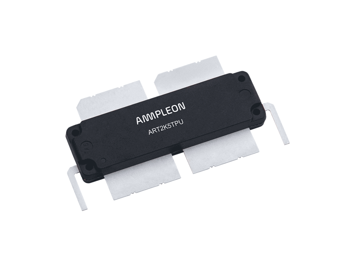
Do you have any plans to build a amplifier with the Ampleon ART2K5TPU if so REALY looking forward to it.
buy the way i am going to buy the 3 kits available ,besides a power supply what else would be necessary to be a COMPLETE amplifier ? thanks
DE Kd6erp
73